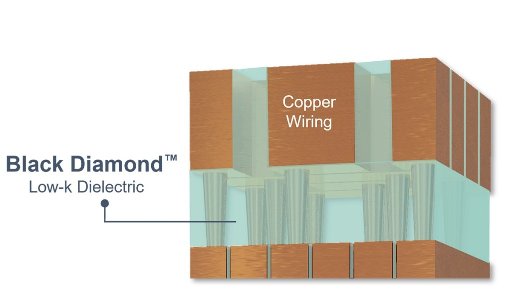
Applied Materials unveils groundbreaking chip wiring advancements, addressing challenges in energy-efficient computing. These innovations enable two-nanometer node manufacturing, reducing resistance in wiring by up to 25% and chip capacitance by 3%. The developments are crucial for logic and memory chip makers, supporting the creation of more powerful and efficient processors.
Key points:
- New materials in chip wiring enable two-nanometer node manufacturing
- Wiring resistance reduced by up to 25%, chip capacitance lowered by 3%
- Innovations support the development of trillion-transistor chips
These advancements are significant as they help maintain the pace of Moore’s Law, which predicts the doubling of components on a chip every couple of years. The chip industry has achieved a three-times improvement every two years over the past 15 years, and these new materials are crucial to continuing this trend.
The innovations in chip wiring and materials engineering are essential for the AI era, which demands more energy-efficient computing. By improving chip performance and reducing power consumption, these advancements will enable the development of more powerful AI processors and graphics processing units. This progress is vital for supporting the growing demands of artificial intelligence and high-performance computing applications.