Overview of Cadence’s Innovation
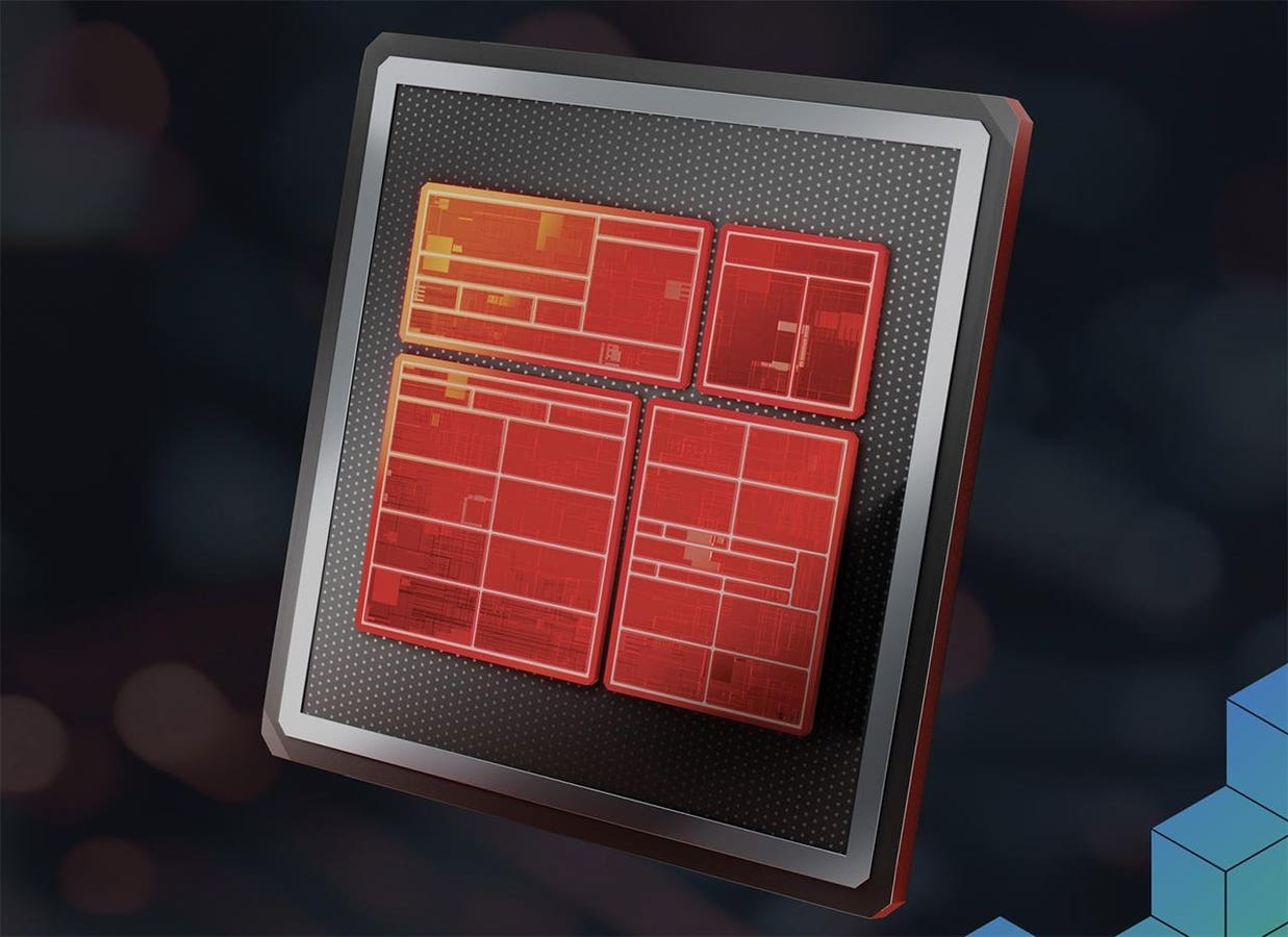
Cadence Design Systems has achieved a significant milestone with its new system chiplet architecture, which aims to enhance the semiconductor industry’s shift towards chiplet-based designs. This architecture is designed to streamline the integration of multiple chiplets into a cohesive system-on-chip (SoC). The system chiplet includes a range of essential components, such as processors and controllers, all interconnected through the Universal Chiplet Interconnect Express (UCIe). The successful silicon bring-up demonstrates Cadence’s commitment to advancing modular silicon platforms.
Key Highlights
- Cadence’s system chiplet successfully initializes LPDDR5X memory at impressive speeds of 9,600 MT/s.
- The validation of UCIe at 32 Gb/s over a 25 mm link showcases robust cross-industry connectivity.
- Modular architectures allow for greater flexibility in design, enabling the mixing of different nodes and functions.
- The system chiplet serves as a reference point for semiconductor developers, reducing risk and design cycles.
Significance in the Semiconductor Landscape
The introduction of Cadence’s system chiplet is crucial as the semiconductor industry faces challenges related to Moore’s Law and rising manufacturing costs. By promoting chiplet designs, Cadence offers a solution that enhances performance and accelerates time to market for diverse applications, particularly in edge and physical-AI markets. The broader adoption of this technology could lead to significant advancements in efficiency and functionality across various sectors, including autonomous systems. The ultimate impact will depend on how well Cadence can engage customers and navigate the complexities of chiplet integration.